
A collaborative team from Lawrence Livermore National Laboratory (LLNL) and Stanford University has unveiled a 3D printing technology capable of cross-scale manufacturing—producing centimeter-sized objects with features as fine as 113 nanometers, smaller than the smallest virus. Published recently in Nature, the research marks a paradigm shift in nanofabrication by solving the industry’s greatest bottleneck: the trade-off between macro-scale size and nano-scale precision.
Traditional two-photon lithography (TPL) is the gold standard for 3D nanoprinting, but it is notoriously slow. Printing a centimeter-scale object with nanoscale detail could previously take weeks. The team, led by LLNL’s Xiaoxing Xia and Stanford’s Jonathan Fan, accelerated this process by replacing the single laser beam with a metalens array.
The researchers developed a system called Metalens Array Two-Photon Lithography, also referred to as MetaLitho3D, which utilizes over 120,000 focused light spots to print simultaneously.
“We have truly achieved 3D nanofabrication at the centimeter scale for the first time,” potentially enabling the printing of complex nanosystems and functional structures, Gu Songyun (pictured) a postdoctoral researcher at LLNL and the lead author of the study, told DeepTech. “Previously, it was like using one carving knife to work slowly; now, 120,000 knives are working at once.” This allows for a printing speed of 120 million voxels per second, several orders of magnitude faster than conventional methods.
Possible applications range from chip manufacturing and large-area neural probes to integrated photonic devices, quantum computing components, and high-energy laser physics.
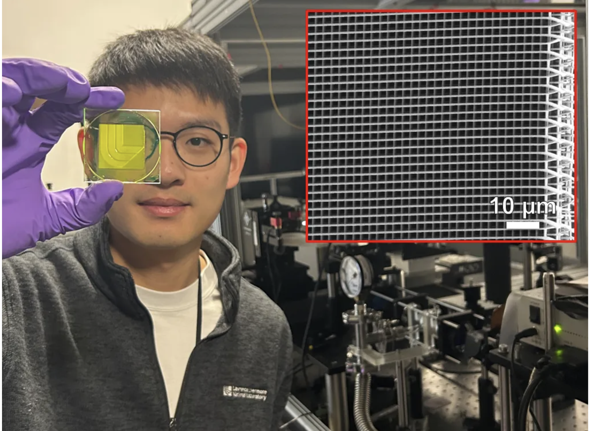
Technical core: the metalens advantage
The breakthrough centers on the use of metalenses — flat, planar lenses surfaced with nanostructures smaller than the wavelength of light. Unlike bulky conventional glass lenses, metalenses are extremely thin and can be manufactured in large formats, arranged in massive arrays, can operate while submerged in resin, and can withstand high-power lasers.
The researchers demonstrated two specific configurations: a 50×50 array for ultra-high-precision tasks; and a 370×350 array (120,000+ lenses) covering 12 square centimeters for high-speed mass production.
By using a spatial light modulator to shape the laser, the team can control the height and “on/off” status of every single light spot. This level of control ensures that despite the massive scale, the deviation in printed line widths is a mere 16.5 nanometers.
Real-world applications
To prove the system’s versatility, the team showcased several groundbreaking applications.
Mass production: they printed 50,000 identical 3D microboats (benchies) in minutes. With the larger array, the system could produce 50 million such microparticles in a single day, a feat previously impossible for nanoprinting.
Gradient-density foam materials: the team fabricated foam structures with precisely controlled density gradients. Such materials are useful in fields including laser-driven proton acceleration, gradient metamaterials, and photonic crystals, but are difficult to manufacture with traditional methods because the density must vary continuously and precisely.
Terahertz metamaterials: terahertz radiation lies between microwave and infrared frequencies but natural materials offer limited control over terahertz waves. The team fabricated complex 3D spirals that were gold-plated to manipulate terahertz waves. These “architected” materials can selectively filter circularly polarized waves, which is vital for next-generation security scanners and biosensing.
Mechanical breakthroughs: the team used the system to test fracture mechanics by printing three different structures into centimeter-scale specimens containing hundreds of thousands of lattice cells. Such experiments would be nearly impossible using conventional nanoprinting. Of the three, they discovered that a chainmail (link) lattice—consisting of interlocking but lacking rigid connections — was significantly tougher than traditional structures. It could stretch nearly six times further than the stiffest lattice before failing, as the stress was distributed across the entire structure rather than a single crack tip.
The future: AI and scale
The ability to print at the centimeter scale with nanometer precision allows for the creation of “cross-scale” systems, from chip manufacturing and neural probes to high-energy laser physics. However, the sheer volume of data generated by 120 million voxels per second presents a new challenge.
“For such a complex system, it is difficult to rely on manual effort for error correction,” Gu said. Because the total print area is hundreds of thousands of times larger than the individual features, no current monitoring system can see the “whole” and the “parts” at the same time. To solve this, the team is currently exploring ways to integrate AI into nanoscale 3D manufacturing to monitor and control the process.
Source: DeepTech
https://mp.weixin.qq.com/s/nbOq-fmk50ZS5DoMqgHFhw?scene=1